The 6502 CPU has an address range of 64K bytes. The upper 1K byte of address space is shared by the RAM, the ROM, Suzy hardware and Mikey hardware. This upper 1K byte of space is divided as tollows:
FFFE, FFFFThe above listed adress ranges (except for FFF8 and FFF9) can, under control of the CPU, have RAM overlayed on them. These overlays are controlled by the bits in the hardware register at FFF9. Both Mikey and Suzy accept a write at those addresses but only Mikey responds to a read.
The remaining 63k bytes are RAM.
These address ranges affect only CPU accesses from Mikey. The video and refresh generators in Mikey and the sprite engine in Suzy see the entire 64K byte range as RAM.
BIG NOTE!!!!! We are done messing around with these addresses. Do not change them anymore!!!
- Legend
(W), (R), (R/W) indicate write only, read only, and read/write capability of a particular address.
Please follow the rules:If an address is read only, DON'T write to it.If an address is write only, DON'T read it.The reset condition is shown with bit 7 on the left (B7......B0). X indicates unchanged by reset.
(U) indicates that it is unsafe to read or write this address without first checking (at a different address) to see if it is available. Please follow the rules. A description of UNSAFE is in the hardware specification.
(CPU), (ENG), (SCB), indicate the usual source of data for this particular address.
CPU = Mikey,
ENG = sprite engine,
SCB = DMA from the RAM based sprite control block. - Memory Map Control
FFF9 = MAPCTL. Memory Map Control
(R/W)Mikey reset = 0,0,0,0,0,0,0,0
(W) Suzy reset x,x,x,x,x,x,x,0
(0nly bit 0 is implemented)B7 = sequential disable. If set, the CPU will always use full cycles (5 ticks min), never a sequential cycle (4 ticks).
B6, B5, B4 = reserved for future use
B3 = FFFA -> FFFF, Vector Space
B2 = FE00 -> FFF7, ROM Space
B1 = FD00 -> FDFF, Mikey Space
B0 = FC00 -> FCFF, Suzy SpaceAll 8 bits are set to 0 at reset. Any address space bit that is set to a 1 will cause its related address space to access RAM instead of the hardware or ROM normally accessed.
FC00 -> FC7F = Sprite Control Block
(R/W) (U)
reset x,x,x,x,x,x,x,x
Even addresses are the LSB.
Any CPU write to an LSB will set the MSB to 0.
| Name | machine | $FCxx | description |
|---|---|---|---|
| L0 | (ENG) | 00,01 | TMPADRL,H Temporary address |
| H0 | (ENG) | 02,03 | TILTACUML,H Accumulator for tilt value |
| L1 | (CPU) | 04,05 | HOFFL,H Offset to H edge of screen |
| H1 | (CPU) | 06,07 | VOFFL,H Offset to V edge of screen |
| L2 | (CPU) | 08.09 | VIDBASL,H Base Address of Video Build Buffer |
| H2 | (CPU) | 0A,0B | COLLBASL,H Base Address of Coll Build Buffer |
| L3 | (ENG) | 0C,0D | VIDADRL,H Current Video Build Address |
| H3 | (ENG) | 0E.0F | COLLADRL H Current Collision Build Address |
| L4 | (SCB) | 10,11 | SCBNEXTL,H Address of Next SCB |
| H4 | (SCB) | 12,13 | SPRDLINEL,H Start of Sprite Data Line Address |
| LS | (SCB) | 14,15 | HPOSSTRTL,H Starting Hpos |
| H5 | (SCB) | 16,17 | VPOSSTRTL,H Starting Vpos |
| L6 | (SCB) | 18,19 | SPRHSIZL,H H Size |
| H6 | (SCB) | 1A,1B | SPRVSIZL,H V Size |
| L7 | (ENG) | 1C,1D | STRETCHL H H Size Adder |
| H7 | (ENG) | 1E,1F | TILTL,H H Position Adder |
| LS | (ENG) | 20,21 | SPRDOFFL,H Offset to Next Sprite Data Line |
| HS | (ENG) | 22,23 | SPRVPOSL,H Current Vpos |
| L9 | (CPU) | 24,25 | COLLOFFL,H Offset to Collision Depository |
| H9 | (ENG) | 26,27 | VSIZACUML,H Vertical Size Accumulator |
| L10 | (CPU) | 28,29 | HSIZOFFL,H Horizontal Size Offset |
| H10 | (CPU) | 2A,2B | VSIZOFFL,H Vertical Size Offset |
| L11 | (ENG) | 2C,2D | SCBADRL,H Address of Current SCB |
| H11 | (ENG) | 2E,2F | PROCADRL,H Current Spr Data Proc Address |
| --- | (ENG) | 30 thru 4F | reserved |
| --- | (ENG) | 50,51 | Do Not Use |
| H4 | (ENG) | 52 | MATHD (12) |
| H4 | (ENG) | 53 | MATHC (13) |
| L5 | (ENG) | 54 | MATHB (14) |
| L5 | (ENG) | 55 | MATHA (15) |
| H5 | (ENG) | 56 | MATHP (16) |
| H5 | (ENG) | 57 | MATHN (17) |
| --- | (ENG) | 58 thru 5F | Do Not Use |
| L8 | (ENG) | 60 | MATHH (20) |
| L8 | (ENG) | 61 | MATHG (21) |
| H8 | (ENG) | 62 | MATHF (22) |
| H8 | (ENG) | 63 | MATHE (23) |
| --- | (ENG) | 64 thru 6B | Do Not Use |
| L11 | (ENG) | 6C | MATHM (2C) |
| L11 | (ENG) | 6D | MATHL (2D) |
| H11 | (ENG) | 6E | MATHK (2E) |
| H11 | (ENG) | 6F | MATHJ (2F) |
| --- | (ENG) | 70 thru 7F | Do Not Use- |
FC80 = SPRCTL0 Sprite Control Bits 0
(W)
(U) reset x,x,x,x,x,x,x,x
B5 = H flip, 0 = not flipped
B4 = V flip, 0 = not flipped
B3 reserved
B2,B1,B0 = Sprite Type
7 -> shadow
6 -> exclusive-or, shadow
5 -> non-collidable
4 -> normal
3 -> boundary
2 -> boundary-shadow
1 -> background-no collision
0 -> background, shadow
FC81 = SPRCTL1 Sprite Control Bits 1
(W)(U)
reset x,x,x,x,x,x,x,x
B6 = Sizing algorithm choice, 0=adder (algo 4), 1=shifter (algo 3)
SET IT T0 ZERO!!!!, algo 3 is broke
B5,B4 = Reloadable depth.
1=Hsize,Vsize.
2=Hsize,Vsize,Stretch.
3=Hsize, Vsize,Stretch, Tilt.
B2 = Skipsprite. 1 skip this sprite, 0=use this sprite.
B1 = Start drawing up (1=up, 0=down)
B0 = Start drawing left (1 left, 0=right)
FC82 = SPRCOLL. Sprite Collision Number
(W)
(U) reset = x,x,x,x,x,x,x,x
B5 = dont collide. 1=dont collide with this sprite.
B4 = 0
B3,B2,B1,B0 = number
FC83 = SPRINIT. Sprite Initialization Bits
(W)(U)
reset x,x,x,x,x,x,x,x
B3 = ac1, B2 = ac2, B1 = ac3, B0 = ac4
Set to '$F3' after at least 100ms after power up and before any sprites are drawn.
FC84 -> FC87 = not yet atlocated
FC88 = SUZYHREV. Suzy Hardware Revision (R)
FC89 = SUZYSREV. Suzy Software Revision
FC8A -> FC8F = not yet atlocated
FC90 = SUZYBUSEN. Suzy Bus Enable (W)
reset = 0
FC91 = SPRG0. Sprite Process Start Bit
(W)
reset = 0
B2= enable everon detector. 1 = enabled.
FC92 = SPRSYS. System Control Bits
(R/W)
(write) reset x,x,x,x,x,x,x,x
B6 = OK to accumulate. 0 = do not accumulate, 1 = yes,accumulate.
B5 = dont collide. 1 = don't collide with any sprites.
B4 = Vstretch. 1 = stretch the v. 0 = Don't play with it, it will grow by itself.
B3 = Lefthand, 0 =normal handed
B2 = Clear the 'unsafeAccess' bit. 1 = clear it. 0 = no change.
B1 = Stop at end of current sprite, 1 request to stop.
B6 = Mathbit. If mult, 1 = accumulator overflow. If div, 1 = div by zero attempted.
B5 = Last carry bit.
B4 = Vstretch.
B3 = Lefthand.
B2 = UnsafeAccess. 1 = Unsafe Access was performed.
B1 = Stop at end of current sprite, 1 = request to stop.
B0 = Sprite process was started and has neither completed nor been stopped.
FC93 -> FCAF = not yet allocated
FCB0 JOYSTICK. Read Joystick and Switches(R)
	If Lefthand=1	If Lefthand=0
	B7 = Joy Up	    (Down)
	B6 = Joy Down	    (Up)
	B5 = Joy Left	    (Right)
	B4 = Joy Right	    (Left)
	B3 = Option 1	    Option 1
	B2 = Option 2	    Option 2
	B1 = Inside	    Inside
	B0 = Outside	    Outside
FCB1 = SWITCHES. Read Other Switches (R)
B6 = 0
B5 = 0
B4 = 0
B3 = 0
B2 = Cart1 I/O Inactive
B1 = Cart0 I/O Inactive
B0 = Pause (was Flablode)
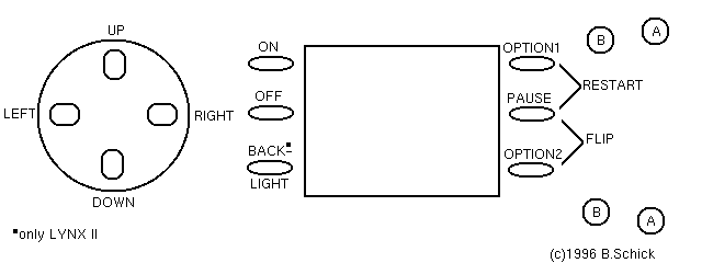
This Picture shows the Normal orientation of the
unit, which according to our previous definition is the
LeftHand orientation. Please realize that this means
that the normal setup is Flip off, and LeftHand
on.
The current agreement is that Pause and Option
1 pressed together will result in the patter of little
rubber feet around the house. Also, Pause and
Option 2 pressed together will be used to indicate a
user request for the Flip function.
FCB2,FCB3 RCART(R/W)
FCB2 uses 'CART0/' as the strobe.
FCB3 uses 'CART1/’ as the strobe.
FCB4-> FCBF = not yet allocated
FCC0 LEDS (W)
reset=0,0,0,0,0,0,0,0
FCC1 Reserved
FCC2 Parallel Port Status(R/W)
reset 0,0,x,x,x,x,x,x
(write)
B6 = paper out, used to signal the device at the other end of the parallel cable.
(read)
When in output mode, B7=1 indicates that an output character is in the data register and awaiting acknowledgement from the device on the other end of the parallel cable. This bit is cleared when that other device accepts the character. In addition, this bit is cleared whenever the direction of the port is changed.
B6 = Hello Handy
FCC3 Parallel Port Data (R/W)
FCC4 Howie (R/W)
FCC5 Reserved
FCC6 -> FCCF = not yet allocated
FCD0 -> FCFF = not yet allocated
Timers
Timers are reset to 0
FD00 -> FD03 Timer channel 0 and Hcount
FD04 -> FD07 Timer channel 1 and mag0a (read current state
of TAPE0 in b7)
FD08 -> FD0B Timer channel 2 and Vcount
FD0C -> FD0F Timer channel 3 and mag0b
FD10 -> FD13 Timer channel 4 and serial rate
FD14 -> FD17 Timer channel 5 and mag1a (read current state
of TAPE1 in b7)
FD18 -> FD1B Timer channel 6
FD1C -> FD1F Timer channel 7 and mag1b
FD00 = TIM0BKUP. HTIMBKUP. Timer 0 backup value
FD01 = TIM0CTLA. HTIMCTL0. Timer 0 static control
FD02 = TIM0CNT. Timer 0 current count
FD03 = TIM0CTLB. Timer 0 dynamic control
FD04 = TIM1BKUP. MAGA. Timer 1 backup vatue
FD05 = TIM1CTLA. Timer 1 static control
FD06 = TIM1CNT. Timer 1 current count
FD07 = TIM1CTLB. Timer 1 dynamic control
FD08 = TIM2BKUP. VTIMBKUP. Timer 2 backup value
FD09 = TIM2CTLA. Timer 2 static control
FD0A = TIM2CNT. Timer 2 current count
FD0B = TIM2CTLB. Timer 2 dynamic control
FD0C = TIM3BKUP.MAGB. Timer 3 backup value
FD0D = TIM3CTLA. Timer 3 static control
FD0E = TIM3CNT. Timer 3 current count
FD0F = TIM3CTLB. Timer 3 dynamic control
FD10 = TIM4BKUP. BAUDBKUP. Timer 4 backup value
FD11 = TIM4CTLA, Timer 4 static control
FD12 = TIM4CNT. Timer 4 current count
FD13 = TIM4CTLB. Timer 4 dynamic control
FD14 = TIM5BKUP. MAGC. Timer 5 backup value
FD15 = TIMSCTLA. Timer 5 static control
FD16 = TIM5CNT. Timer 5 current count
FD17 = TIMSCTLB. Timer 5 dynamic control
FD18 = TIM6BKUP. Timer 6 backup value
FD19 = TIM6CTLA. Timer 6 static control
FD1A = TIM6CNT. Timer 6 current count
FD1B = TIM6CTLB. Timer 6 dynamic control
FD1C = TIM7BKUP.MAGD. Timer 7 backup value
FD1D = TIM7CTLA. Timer 7 static control
FD1E = TIM7CNT. Timer 7 current count
FD1F = TIM7CTLB. Timer 7 dynamic control
| xxx0 | HEX | 7 | 6 | 5 | 4 | 3 | 2 | 1 | 0 |
|---|---|---|---|---|---|---|---|---|---|
| backup value | |||||||||
| xxx1 | HEX | 7 | 6 | 5 | 4 | 3 | 2 | 1 | 0 |
| control bits | |||||||||
| Enable interrupt | $80 | 1 | . | . | . | . | . | . | . |
| Reset Timer Done | $40 | . | 1 | . | . | . | . | . | . |
| Unused in timers 0,2,4,6 / Magmode in timers 1,3,5,7 | $20 | . | . | 1 | . | . | . | . | . |
| Enable reload | $10 | . | . | . | 1 | . | . | . | . |
| Enable count | $08 | . | . | . | . | 1 | . | . | . |
| clock select | |||||||||
| linking | $07 | . | . | . | . | . | 1 | 1 | 1 |
| 64us | $06 | . | . | . | . | . | 1 | 1 | 0 |
| 32us | $05 | . | . | . | . | . | 1 | 0 | 1 |
| 16us | $04 | . | . | . | . | . | 1 | 0 | 0 |
| 8us | $03 | . | . | . | . | . | 0 | 1 | 1 |
| 4us | $02 | . | . | . | . | . | 0 | 1 | 0 |
| 2us | $01 | . | . | . | . | . | 0 | 0 | 1 |
| 1us | $00 | . | . | . | . | . | 0 | 0 | 0 |
| xxx2 | HEX | 7 | 6 | 5 | 4 | 3 | 2 | 1 | 0 |
| current value | |||||||||
| xxx3 | HEX | 7 | 6 | 5 | 4 | 3 | 2 | 1 | 0 |
| more control bits | |||||||||
| Timer Done(1) | $08 | . | . | . | . | 1 | . | . | . |
| Last clock | $04 | . | . | . | . | . | 1 | . | . |
| Borrow in | $02 | . | . | . | . | . | . | 1 | . |
| Borrow out | $01 | . | . | . | . | . | . | . | 1 |
(1) It is set on time out, reset with the reset timer done bit (xxx1, B6)
Audio
Audio are reset to 0, all are read/write
FD20 -> FD27 Audio channel 0, links from timer 7
FD28 -> FD2F Audio channel 1, links from audio timer 0
FD30 -> FD37 Audio channel 2, links from audio timer 1
FD38 -> FD3F Audio channel 3, links trom audio timer 2
FD20 = 8 bit. 2's Complement Volume Control
00000001 is the same volume as 11111111, but opposite phase.
FD21 = Shift Register Feedback Enable
B6=feedback bit 10
B5=feedback bit 5
B4=feedback bit 4
B3=feedback bit 3
B2=feedback bit 2
B1=feedback bit 1
B0=feedback bit 0
FD22 = Audio Output Value
In normal mode, shift reg 0 = 1: contains value of volume register.
In integrate mode, shift reg 0 = 0: subtract volume register from output.
In integrate mode, shift reg 0 = 1: add volume register to output.
note that there is hardware clipping at max and min (ff,00).
FD23 = Lower 8 Bits of Shift Register
FD24 = Audio Timer Backup Value
FD25 = Audio Control Bits
B6=reset timer done
B5=enable integrate mode
B4=enable reload
B3=enable count
B2,B1,B0=clock select
6 = 64 us
5 = 32 us
4 = 16 us
3 = 8 us
2 = 4 us
1 = 2 us
0 = 1 us
FD26 = Audio Counter
FD27 = Other Audio Bits
B6=shift register bit 10
B5=shift register bit 9
B4=shift register bit 8
B3=for Glenn to know and you to find out
B2=last clock state (0->1 causes count)
B1=borrow in (1 causes count)
B0=borrow out (count=0 and borrow in)
FD40 -> FD4F = not yet altocated
FD50 = MSTERE0(* R/W)
reset 0,0,0,0,0,0,0,0
*Note:
Write-only on Howards
B7 = Audio Channel 3 -> Left Ear
B6 = Audio Channel 2 -> Left Ear
B5 = Audio Channel 1 -> Left Ear
B4 = Audio Channel 0 -> Left Ear
B3 = Audio Channel 3 -> Right Ear
B2 = Audio Channel 2 -> Right Ear
B1 = Audio Channel 1 -> Right Ear
B0 = Audio Channel 0 -> Right Ear
FD51 -> FD7F = not yet allocated
Misc
FD80 = INTRST.Interrupt Poll 0, (R/W)
reset = 0,0,0,0,0,0,0,0
FD81 INTSET. Interrupt Poll 1, (R/W)
reset = 0,0,0,0,0,0,0,0
B7 = timer 7
B6 = timer 6
B5 = timer 5
B4 = serial interupt
B3 = timer 3
B2 = timer 2 (vertical line counter)
B1 = timer 1
B0 = timer 0 (horizontal line timer)
FD82 -> FD83 = not yet allocated
FD84 = MAGRDY0.Mag Tape Channel 0 ready
bit.(R)
reset = x
FD85 = MAGRDY1. Mag Tape Channel 1 ready
bit.(R)
reset = x
FD86 AUDIN. Audio In.(R)
reset = b7,0,0,0,0,0,0,0
FD87 = SYSCTL1.Control Bits.(W)
reset x,x,x,x,x,x,1,0
B0= Cart Address Strobe (also counter reset) (was MotorOn)
FD88 = MIKEYHREV.Mikey Hardware
Revision(R)
FD89 = MIKEYSREV.Mikey Software Revision(W)
FD8A = IODIR.Mikey Parallel I/O Data
Direction (W)
reset = 0,0.0.0,0,0,0,0
0=input, 1= output,
FD8B = IODAT.Mikey Parallel Data(sort of a
R/W)
8 bits of general purpose I/O data
B6 = NC
B5 = NC
B4 = audin input
B3 = rest output
B2 = noexp input
B1 = Cart Address Data output (0 turns cart power on)
B0 = External Power input
(note, ROM sets it to output, you must set it to input)
Note that some lines are used for several functions,
please read the spec.
Also note that only the lines that are set to input are
actually valid for reading.
--READ THE SPEC----
FD8C = SERCTL. Serial Control
Register.(R/W)
reset 0,0,0,0,0,0,0,0
(write)
B6 = RXINTEN receive interrupt enable
B5 = 0 (for future compatibility)
B4 = PAREN xmit parity enable (if 0, PAREVEN is the bit sent)
B3 = RESETERR reset all errors
B2 = TXOPEN 1 open collector driver, 0 = TTL driver
B1 = TXBRK send a break (for as long as the bit is set)
B0 = PAREVEN send/rcv even parity
(read)
B6 = RXRDY receive character ready
B5 = TXEMPTY transmitter totaiy done
B4 = PARERR received parity error
B3 = 0VERRUN received overrun error
B2 = FRAMERR received framing error
B1 = RXBRK break recieved (24 bit periods)
B0 = PARBIT 9th bit
FD8D = SERDAT. Serial Data .(R/W)
reset = x,x,x,x,x,x,x,x
FD8E -> FD8F = not yet allocated
FD90 = SDONEACK. Suzy Done Acknowledge,
(W)
reset = 0 (not acked)
FD91 = CPUSLEEP. CPU Bus Request Disable(W)
The setting of the flip flop is described in the hardware specification.
FD92 = DISPCTL. Video Bus Reguest Enable,
(W)
reset = 0
B3 = color, 1=color, 0=monochrome
B2 = fourbit, 1=4 bit mode, 0=2 bit mode
B1 = 1=flip, 0 normal
B0 = 1=enable video DMA, 0=disable
FD93 = PBKUP. Magic 'P' count, (W)
reset = x,x,x,x,x,x,x,x
At 60 Hz, 'PBKUP' = 41. (0x29)
FD94 ->FD95= DISPADRL,H . Start Address
of Video Disptay, (W)
reset x,x,x,x,x,x,x,x
DISPADRL (FD94) is lower 8 bits of display address
with the bottom 2 bit ignored by the hardware The address of the upper left corner of a display buffer must always have '00' in the bottom 2 bits.
FD96 -> FD9B = not yet altocated
FD9C = Mtest0,(W)
reset 0,0,0,0,0,0,0,0
B6 = ATtest
B5 = XCLKEN
B4 = UARTturbo
B3 = ROMsel
B2 = ROMtest
B1 = Mtest
B0 = CPUtest
Setting UARTturbo switches the baudrate to 1MBd!
FD9D = Mtest1,(W)
reset x,0,0,0,0.0,0,0
B6 = Pcnt16
B5 = REFcnt16
B4 = VIDtrig
B3 = REFtrig
B2 = VIDdmaDIS
B1 = REFfast
B0 = REFdis
FD9E = Mtest2,(W)
reset = x,x,x,0,0,0,0,0
B4 = Vstrobe
B3 = Vzero
B2 = H120
B1 = Hzero
B0 = Vblankef
FDA0 -> FDAF =Green Color map,
(R/W)
reset x,x,x,x,x,x,x,x
B3->B0 = green
FDB0 -> FDBF =Blue and Red color
map,
(R/W) reset x,x,x,x,x,x,x,x
B3->B0 = red
	FDA0 = GREEN0	 FDA8 = GREEN8
	FDA1 = GREEN1	 FDA9 = GREEN9
	FDA2 = GREEN2	 FDAA = GREENA
	FDA3 = GREEN3	 FDAB = GREENB
	FDA4 = GREEN4	 FDAC = GREENC
	FDAS = GREEN5	 FDAD = GREEND
	FDA6 = GREEN6	 FDAE = GREENE
	FDA7 = GREEN7	 FDAF = GREENF

	FDB0 = BLUERED0	 FDB8 = BLUERED8
	FDB1 = BLUERED1	 FDB9 = BLUERED9
	FDB2 = BLUERED2	 FDBA = BLUEREDA
	FDB3 = BLUERED3	 FDBB = BLUEREDB
	FDB4 = BLUERED4	 FDBC = BLUEREDC
	FDB5 = BLUERED5	 FDBD = BLUEREDD
	FDB6 = BLUERED6	 FDBE = BLUEREDE
	FDB7 = BLUERED7	 FDBF = BLUEREDF
FDC0 -> FDCF = not yet allocated
FDD0 -> FDFF = not yet allocated
| JOYPAD ($FCB0) |
HEX | 7 | 6 | 5 | 4 | 3 | 2 | 1 | 0 | SWITCHES ($FCB1) |
HEX | 7 | 6 | 5 | 4 | 3 | 2 | 1 | 0 | |
|---|---|---|---|---|---|---|---|---|---|---|---|---|---|---|---|---|---|---|---|---|
| JOYSTICK bit definition | SWITCHES bit definitions | |||||||||||||||||||
| JOY_DOWN | $80 | 1 | . | . | . | . | . | . | . | . | ||||||||||
| JOY_UP | $40 | . | 1 | . | . | . | . | . | . | |||||||||||
| JOY_RIGHT | $20 | . | . | 1 | . | . | . | . | . | |||||||||||
| JOY_LEFT | $10 | . | . | . | 1 | . | . | . | . | |||||||||||
| OPTION1 | $08 | . | . | . | . | 1 | . | . | . | |||||||||||
| OPTION2 | $04 | . | . | . | . | . | 1 | . | . | CART1_STROBE | $04 | . | . | . | . | . | 1 | . | . | |
| B_BUTTON | $02 | . | . | . | . | . | . | 1 | . | CART0_STROBE | $02 | . | . | . | . | . | . | 1 | . | |
| A_BUTTON | $01 | . | . | . | . | . | . | . | 1 | PAUSE_BUTTON | $01 | . | . | . | . | . | . | . | 1 | |
| SPRCTL0 ($FC80) |
HEX | 7 | 6 | 5 | 4 | 3 | 2 | 1 | 0 | SPRCTL1 ($FC81) |
HEX | 7 | 6 | 5 | 4 | 3 | 2 | 1 | 0 | ||
|---|---|---|---|---|---|---|---|---|---|---|---|---|---|---|---|---|---|---|---|---|---|
| Bits-per-pixel definitions | Sprite control 1 bit definitions | ||||||||||||||||||||
| ONE PER PIXEL | $00 | 0 | 0 | . | . | . | . | . | . | LITERAL | $80 | 1 | . | . | . | . | . | . | . | ||
| TWO PER PIXEL | $40 | 0 | 1 | . | . | . | . | . | . | ALGO 3(1) | $40 | . | 1 | . | . | . | . | . | . | ||
| THREE PER PIXEL | $80 | 1 | 0 | . | . | . | . | . | . | Sprite control 1 bit definitions | |||||||||||
| FOUR PER PIXEL | $C0 | 1 | 1 | . | . | . | . | . | . | RELOAD NONE | $00 | . | . | 0 | 0 | . | . | . | . | ||
| More sprite control 0 it definitions | RELOAD HV | $10 | . | . | 0 | 1 | . | . | . | . | |||||||||||
| HFLIP | $20 | . | . | 1 | . | . | . | . | . | RELOAD HVS | $20 | . | . | 1 | 0 | . | . | . | . | ||
| VFLIP | $10 | . | . | . | 1 | . | . | . | . | RELOAD HVST | $30 | . | . | 1 | 1 | . | . | . | . | ||
| Sprite types | More sprite control 1 it definitions | ||||||||||||||||||||
| SHADOW SPRITE | $07 | . | . | . | . | . | 1 | 1 | 1 | REUSE PALETTE | $08 | . | . | . | . | 1 | . | . | . | ||
| XOR SPRITE | $06 | . | . | . | . | . | 1 | 1 | 0 | SKIP SPRITE | $04 | . | . | . | . | . | 1 | . | . | ||
| NONCOLL SPRITE | $05 | . | . | . | . | . | 1 | 0 | 1 | DRAW UP | $02 | . | . | . | . | . | . | 1 | . | ||
| NORMAL SPRITE | $04 | . | . | . | . | . | 1 | 0 | 0 | DRAW LEFT | $01 | . | . | . | . | . | . | 0 | 1 | ||
| BOUNDARY SPRITE | $03 | . | . | . | . | . | 0 | 1 | 1 | . | |||||||||||
| BSHADOW SPRITE | $02 | . | . | . | . | . | 0 | 1 | 0 | ||||||||||||
| BACKNONCOLL SPR | $01 | . | . | . | . | . | 0 | 0 | 1 | ||||||||||||
| BACKGROUND SPR | $00 | . | . | . | . | . | 0 | 0 | 0 | ||||||||||||
(1)ALGO 3 is broken !
| SPRGO ($FC91) |
HEX | 7 | 6 | 5 | 4 | 3 | 2 | 1 | 0 |
|---|---|---|---|---|---|---|---|---|---|
| EVER_ON | $04 | . | . | . | . | . | 1 | . | . |
| SPRITE_GO | $01 | . | . | . | . | . | . | . | 1 |
| SPRSYS ($FC92)WRITE |
HEX | 7 | 6 | 5 | 4 | 3 | 2 | 1 | 0 | SPRSYS ($FC92)READ |
HEX | 7 | 6 | 5 | 4 | 3 | 2 | 1 | 0 | |
|---|---|---|---|---|---|---|---|---|---|---|---|---|---|---|---|---|---|---|---|---|
| SIGNMATH | $80 | 1 | . | . | . | . | . | . | . | MATHWORKING | $80 | 1 | . | . | . | . | . | . | . | |
| ACCUMULATE | $40 | . | 1 | . | . | . | . | . | . | MATHWARNING | $40 | . | 1 | . | . | . | . | . | . | |
| NO_COLLIDE | $20 | . | . | 1 | . | . | . | . | . | MATHCARRY | $20 | . | . | 1 | . | . | . | . | . | |
| VSTRETCH | $10 | . | . | . | 1 | . | . | . | . | VSTRETCHING | $10 | . | . | . | 1 | . | . | . | . | |
| LEFTHAND | $08 | . | . | . | . | 1 | . | . | . | LEFTHANDED | $08 | . | . | . | . | 1 | . | . | . | |
| CLR_UNSAFE | $04 | . | . | . | . | . | 1 | . | . | UNSAFE_ACCESS | $04 | . | . | . | . | . | 1 | . | . | |
| SPRITESTOP | $02 | . | . | . | . | . | . | 1 | . | SPRITETOSTOP | $02 | . | . | . | . | . | . | 1 | . | |
| SPRITEWORKING | $01 | . | . | . | . | . | . | . | 1 | |||||||||||
| MAPCNTL ($FFF9) |
HEX | 7 | 6 | 5 | 4 | 3 | 2 | 1 | 0 |
|---|---|---|---|---|---|---|---|---|---|
| MAPCTL flag definitions | |||||||||
| HIGH SPEED | $80 | 1 | . | . | . | . | . | . | . |
| VECTOR SPACE | $08 | . | . | . | . | 1 | . | . | . |
| ROM SPACE | $04 | . | . | . | . | . | 1 | . | . |
| MIKEY SPACE | $02 | . | . | . | . | . | . | 1 | . |
| SUZY SPACE | $01 | . | . | . | . | . | . | . | 1 |
[CONTENTS]
HOME
(c) 42Bastian Schick last modified 01/02/23